- 您现在的位置:买卖IC网 > Sheet目录478 > MMDF1N05ER2G (ON Semiconductor)MOSFET N-CHAN DUAL 2A 50V 8SOIC
MMDF1N05E, MVDF1N05E
1200
1000
V GS
C iss
C rss
0
V DS
T J = 25 ° C
12
10
V DS = 25 V
I D = 1.2 A
800
600
V DS = 0
V GS = 0
8
6
400
200
C iss
C oss
C rss
4
2
0
20
15
10
5
0
5 10 15
20
25
0
0
2
4
6
8
10
12
14
16
GATE-TO-SOURCE OR DRAIN-TO-SOURCE VOLTAGE (VOLTS)
Figure 7. Capacitance Variation
Q g , TOTAL GATE CHARGE (nC)
Figure 8. Gate Charge versus
Gate ? To ? Source Voltage
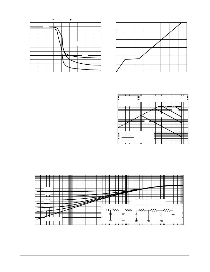
SAFE OPERATING AREA INFORMATION
Forward Biased Safe Operating Area
The FBSOA curves define the maximum drain ? to ? source
voltage and drain current that a device can safely handle
when it is forward biased, or when it is on, or being turned
on. Because these curves include the limitations of
simultaneous high voltage and high current, up to the rating
100
10
1
V GS = 20 V
SINGLE PULSE
T C = 25 ° C
Mounted on 2 ″ sq. FR4 board (1 ″ sq. 2 oz. Cu 0.06 ″
thick single sided) with one die operating, 10s max.
10 m s
100 m s
10 ms
dc
of the device, they are especially useful to designers of linear
systems. The curves are based on a case temperature of 25 ° C
and a maximum junction temperature of 150 ° C. Limitations
for repetitive pulses at various case temperatures can be
determined by using the thermal response curves. ON
Semiconductor Application Note, AN569, “Transient
Thermal Resistance ? General Data and Its Use” provides
detailed instructions.
0.1
0.01
0.1
R DS(on) LIMIT
THERMAL LIMIT
PACKAGE LIMIT
1 10
V DS , DRAIN-TO-SOURCE VOLTAGE (VOLTS)
Figure 9. Maximum Rated Forward Biased
100
Safe Operating Area
10
1
D = 0.5
0.2
0.1
0.1
0.05
Normalized to q ja at 10s.
0.02
Chip
0.0175 W
0.0710 W
0.2706 W
0.5776 W
0.7086 W
0.01
0.01
SINGLE PULSE
0.0154 F
0.0854 F
0.3074 F
1.7891 F
107.55 F
Ambient
0.001
1.0E-05
1.0E-04
1.0E-03
1.0E-02
1.0E-01
1.0E+00
1.0E+01
1.0E+02
1.0E+03
t, TIME (s)
Figure 10. Thermal Response
http://onsemi.com
4
发布紧急采购,3分钟左右您将得到回复。
相关PDF资料
MMDF2C03HDR2G
MOSFET N/P-CHAN 2A 30V 8SOIC
MMDF2N02ER2G
MOSFET N-CHAN DUAL 2A 25V 8SOIC
MMDF2P02ER2G
MOSFET PWR P-CH 25V 2.5A 8-SOIC
MMDF2P02HDR2G
MOSFET P-CH DUAL 3.3A 20V 8SOIC
MMDF3N02HDR2G
MOSFET PWR P-CH 20V 3.8A 8-SOIC
MMDF3N04HDR2G
MOSFET N-CH DUAL 3.4A 40V 8SOIC
MMDFS6N303R2
MOSFET N-CH 30V 6A 8-SOIC
MMFT5P03HDT1
MOSFET P-CH 30V 3.7A SOT223
相关代理商/技术参数
MMDF1N05ER2G
制造商:ON Semiconductor 功能描述:MOSFET
MMDF2C01HD
制造商:MOTOROLA 制造商全称:Motorola, Inc 功能描述:COMPLEMENTARY DUAL TMOS POWER FET 2.0 AMPERES 12 VOLTS
MMDF2C02E
制造商:MOTOROLA 制造商全称:Motorola, Inc 功能描述:COMPLEMENTARY DUAL TMOS POWER FET 2.5 AMPERES 25 VOLTS
MMDF2C02HD
制造商:MOTOROLA 制造商全称:Motorola, Inc 功能描述:COMPLEMENTARY DUAL TMOS POWER FET 2.0 AMPERES 20 VOLTS
MMDF2C02HDR2
制造商:ON Semiconductor 功能描述: 制造商:Motorola Inc 功能描述:
MMDF2C03HD
制造商:MOTOROLA 制造商全称:Motorola, Inc 功能描述:COMPLEMENTARY DUAL TMOS POWER FET 2.0 AMPERES 30 VOLTS
MMDF2C03HDR2
功能描述:MOSFET 30V 2A RoHS:否 制造商:STMicroelectronics 晶体管极性:N-Channel 汲极/源极击穿电压:650 V 闸/源击穿电压:25 V 漏极连续电流:130 A 电阻汲极/源极 RDS(导通):0.014 Ohms 配置:Single 最大工作温度: 安装风格:Through Hole 封装 / 箱体:Max247 封装:Tube
MMDF2C03HDR2G
功能描述:MOSFET COMP S08C 30V 4.1A 70mOhm RoHS:否 制造商:STMicroelectronics 晶体管极性:N-Channel 汲极/源极击穿电压:650 V 闸/源击穿电压:25 V 漏极连续电流:130 A 电阻汲极/源极 RDS(导通):0.014 Ohms 配置:Single 最大工作温度: 安装风格:Through Hole 封装 / 箱体:Max247 封装:Tube
