- 您现在的位置:买卖IC网 > Sheet目录478 > MMDF1N05ER2G (ON Semiconductor)MOSFET N-CHAN DUAL 2A 50V 8SOIC
�� �
�
�MMDF1N05E,� MVDF1N05E�
�1200�
�1000�
�V� GS�
�C� iss�
�C� rss�
�0�
�V� DS�
�T� J� =� 25� °� C�
�12�
�10�
�V� DS� =� 25� V�
�I� D� =� 1.2� A�
�800�
�600�
�V� DS� =� 0�
�V� GS� =� 0�
�8�
�6�
�400�
�200�
�C� iss�
�C� oss�
�C� rss�
�4�
�2�
�0�
�20�
�15�
�10�
�5�
�0�
�5� 10� 15�
�20�
�25�
�0�
�0�
�2�
�4�
�6�
�8�
�10�
�12�
�14�
�16�
�GATE-TO-SOURCE� OR� DRAIN-TO-SOURCE� VOLTAGE� (VOLTS)�
�Figure� 7.� Capacitance� Variation�
�Q� g� ,� TOTAL� GATE� CHARGE� (nC)�
�Figure� 8.� Gate� Charge� versus�
�Gate� ?� To� ?� Source� Voltage�
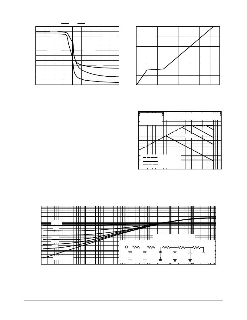
�SAFE� OPERATING� AREA� INFORMATION�
�Forward� Biased� Safe� Operating� Area�
�The� FBSOA� curves� define� the� maximum� drain� ?� to� ?� source�
�voltage� and� drain� current� that� a� device� can� safely� handle�
�when� it� is� forward� biased,� or� when� it� is� on,� or� being� turned�
�on.� Because� these� curves� include� the� limitations� of�
�simultaneous� high� voltage� and� high� current,� up� to� the� rating�
�100�
�10�
�1�
�V� GS� =� 20� V�
�SINGLE� PULSE�
�T� C� =� 25� °� C�
�Mounted� on� 2� ″� sq.� FR4� board� (1� ″� sq.� 2� oz.� Cu� 0.06� ″�
�thick� single� sided)� with� one� die� operating,� 10s� max.�
�10� m� s�
�100� m� s�
�10 ms�
�dc�
�of� the� device,� they� are� especially� useful� to� designers� of� linear�
�systems.� The� curves� are� based� on� a� case� temperature� of� 25� °� C�
�and� a� maximum� junction� temperature� of� 150� °� C.� Limitations�
�for� repetitive� pulses� at� various� case� temperatures� can� be�
�determined� by� using� the� thermal� response� curves.� ON�
�Semiconductor� Application� Note,� AN569,� “Transient�
�Thermal� Resistance� ?� General� Data� and� Its� Use”� provides�
�detailed� instructions.�
�0.1�
�0.01�
�0.1�
�R� DS(on)� LIMIT�
�THERMAL� LIMIT�
�PACKAGE� LIMIT�
�1� 10�
�V� DS� ,� DRAIN-TO-SOURCE� VOLTAGE� (VOLTS)�
�Figure� 9.� Maximum� Rated� Forward� Biased�
�100�
�Safe� Operating� Area�
�10�
�1�
�D = 0.5�
�0.2�
�0.1�
�0.1�
�0.05�
�Normalized to� q� ja at 10s.�
�0.02�
�Chip�
�0.0175� W�
�0.0710� W�
�0.2706� W�
�0.5776� W�
�0.7086� W�
�0.01�
�0.01�
�SINGLE PULSE�
�0.0154� F�
�0.0854� F�
�0.3074� F�
�1.7891� F�
�107.55� F�
�Ambient�
�0.001�
�1.0E-05�
�1.0E-04�
�1.0E-03�
�1.0E-02�
�1.0E-01�
�1.0E+00�
�1.0E+01�
�1.0E+02�
�1.0E+03�
�t,� TIME� (s)�
�Figure� 10.� Thermal� Response�
�http://onsemi.com�
�4�
�发布紧急采购,3分钟左右您将得到回复。
相关PDF资料
MMDF2C03HDR2G
MOSFET N/P-CHAN 2A 30V 8SOIC
MMDF2N02ER2G
MOSFET N-CHAN DUAL 2A 25V 8SOIC
MMDF2P02ER2G
MOSFET PWR P-CH 25V 2.5A 8-SOIC
MMDF2P02HDR2G
MOSFET P-CH DUAL 3.3A 20V 8SOIC
MMDF3N02HDR2G
MOSFET PWR P-CH 20V 3.8A 8-SOIC
MMDF3N04HDR2G
MOSFET N-CH DUAL 3.4A 40V 8SOIC
MMDFS6N303R2
MOSFET N-CH 30V 6A 8-SOIC
MMFT5P03HDT1
MOSFET P-CH 30V 3.7A SOT223
相关代理商/技术参数
MMDF1N05ER2G
制造商:ON Semiconductor 功能描述:MOSFET
MMDF2C01HD
制造商:MOTOROLA 制造商全称:Motorola, Inc 功能描述:COMPLEMENTARY DUAL TMOS POWER FET 2.0 AMPERES 12 VOLTS
MMDF2C02E
制造商:MOTOROLA 制造商全称:Motorola, Inc 功能描述:COMPLEMENTARY DUAL TMOS POWER FET 2.5 AMPERES 25 VOLTS
MMDF2C02HD
制造商:MOTOROLA 制造商全称:Motorola, Inc 功能描述:COMPLEMENTARY DUAL TMOS POWER FET 2.0 AMPERES 20 VOLTS
MMDF2C02HDR2
制造商:ON Semiconductor 功能描述: 制造商:Motorola Inc 功能描述:
MMDF2C03HD
制造商:MOTOROLA 制造商全称:Motorola, Inc 功能描述:COMPLEMENTARY DUAL TMOS POWER FET 2.0 AMPERES 30 VOLTS
MMDF2C03HDR2
功能描述:MOSFET 30V 2A RoHS:否 制造商:STMicroelectronics 晶体管极性:N-Channel 汲极/源极击穿电压:650 V 闸/源击穿电压:25 V 漏极连续电流:130 A 电阻汲极/源极 RDS(导通):0.014 Ohms 配置:Single 最大工作温度: 安装风格:Through Hole 封装 / 箱体:Max247 封装:Tube
MMDF2C03HDR2G
功能描述:MOSFET COMP S08C 30V 4.1A 70mOhm RoHS:否 制造商:STMicroelectronics 晶体管极性:N-Channel 汲极/源极击穿电压:650 V 闸/源击穿电压:25 V 漏极连续电流:130 A 电阻汲极/源极 RDS(导通):0.014 Ohms 配置:Single 最大工作温度: 安装风格:Through Hole 封装 / 箱体:Max247 封装:Tube